Announcement of Exhibition at “SEMICON Japan 2025”
Innovating Next-Generation Power Semiconductor Processing: Hands-on Exhibits and Technical Reveal of the New “DIALOGIC PLUS+” System
Mitsuboshi Diamond Industrial Co., Ltd. (Headquarters: Settsu City, Osaka; President: Masaki Wakabayashi) is pleased to announce our participation in “SEMICON Japan 2025,” the international exhibition for semiconductor packaging and manufacturing technology, to be held at Tokyo Big Sight from Wednesday, December 17 to Friday, December 19, 2025.
Based on the “brittle material processing technology” we have cultivated over 90 years since our founding, MDI has recently been promoting technological innovation in the semiconductor field, particularly in the processing of compound semiconductors such as SiC (Silicon Carbide).
At this exhibition, we will feature exhibits where visitors can physically experience the utility of our core technology, the “Scribe & Break (SnB) method.” Furthermore, we will unveil the technical details of our latest wafer singulation system for the first time.
[Main Exhibits]
1. [Hands-on Exhibit] Experience the Mechanism of the Scribe & Break (SnB) Method
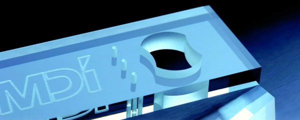
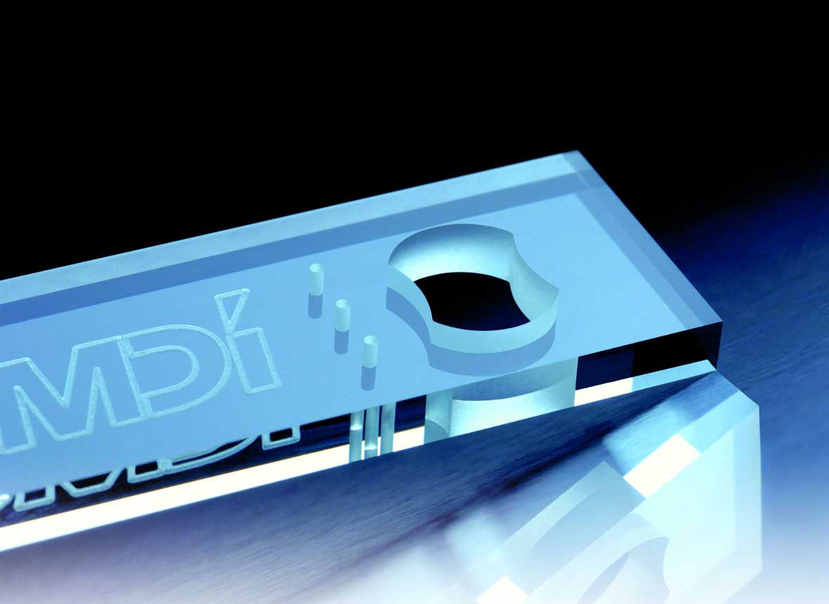
We will set up a special corner where you can understand the mechanism of our proprietary “Scribe & Break (SnB) method”—which differs fundamentally from conventional dicing (sawing)—through an actual breaking experience.
The SnB method is a technology where a line (scribe) is drawn on the material surface using a diamond cutter or similar tool, and stress is applied to break (singulate) the material.
- Completely Dry Process: Eliminates the use of water, significantly reducing environmental impact.
- Narrow Kerf: Generates no cutting waste (swarf), allowing for the waste-free utilization of expensive semiconductor materials.
- High Speed & High Quality: Achieves clean edges with minimal cracks and overwhelming processing speed.
We invite you to experience the true value of this technology at the venue, which simultaneously realizes “environmental performance,” “cost reduction,” and “productivity improvement” in semiconductor device manufacturing.
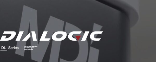
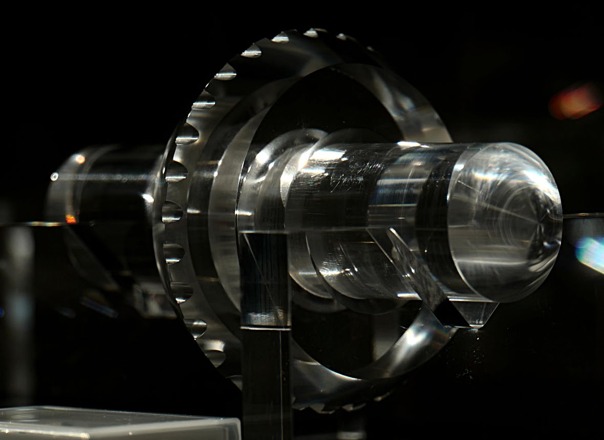
2. New SiC Wafer Singulation System “DIALOGIC PLUS+”: Technical and Configuration Debut
We will introduce the full scope of the “DIALOGIC PLUS+,” a new model joining our well-received “DIALOGIC Series” of semiconductor wafer singulation systems.
In this exhibit, we will be the first to disclose the equipment configuration and technical specifications designed to achieve even higher precision and efficiency for high-hardness, hard-to-cut materials such as SiC wafers, for which demand is rapidly increasing.
While inheriting the “Eco-friendly and lean” features of the conventional DIALOGIC series, our technical staff will use panel displays to explain specific solutions that contribute to productivity improvement, including advanced process conditions and support for automation. Please utilize this opportunity for preliminary consultations regarding implementation.
[Event Overview]
- Exhibition Name: SEMICON Japan 2025
- Dates: Wednesday, December 17 – Friday, December 19, 2025
- Time: 10:00 – 17:00
- Venue: Tokyo Big Sight
- MDI Booth: East Hall 6, E6708
- Official Website: https://www.semiconjapan.org/en/
About Mitsuboshi Diamond Industrial
Under the corporate philosophy of “Walking with an Eye on the Future,” MDI has expanded its scope from glass processing technology to semiconductors, electronic components, and next-generation solar cells (Perovskite). By consistently handling everything from the development of tools utilizing our unique processing technologies to the manufacturing of equipment, we continue to provide optimal innovations for our customers’ manufacturing processes.
We look forward to welcoming you to our booth.
[Contact Information]
Mitsuboshi Diamond Industrial Co., Ltd.
URL: https://www.mitsuboshidiamond.com/
Inquiry Form: https://www.mitsuboshidiamond.com/contact/