Announces New Semiconductor Wafer Singulation System “DIALOGIC Plus+”
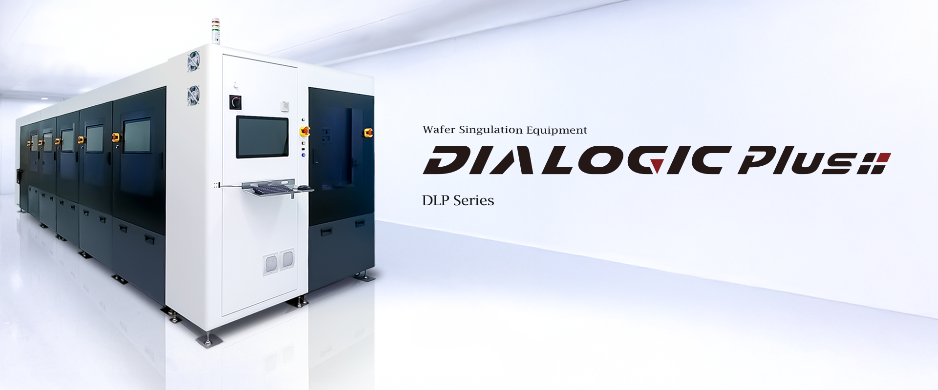
Announces New Semiconductor Wafer Singulation System “DIALOGIC Plus+”
Achieves flexible customization to meet customers’ production needs through modularized system units.
Mitsuboshi Diamond Industrial Co., Ltd. (HQ: Settsu City, Osaka; President CEO: Masaki Wakabayashi) is pleased to announce the development and launch of its new wafer singulation system, “DIALOGIC Plus+” as the latest addition to the DIALOGIC series.
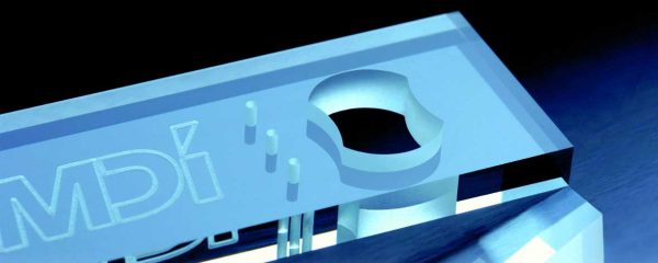
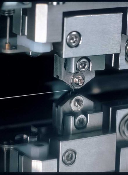
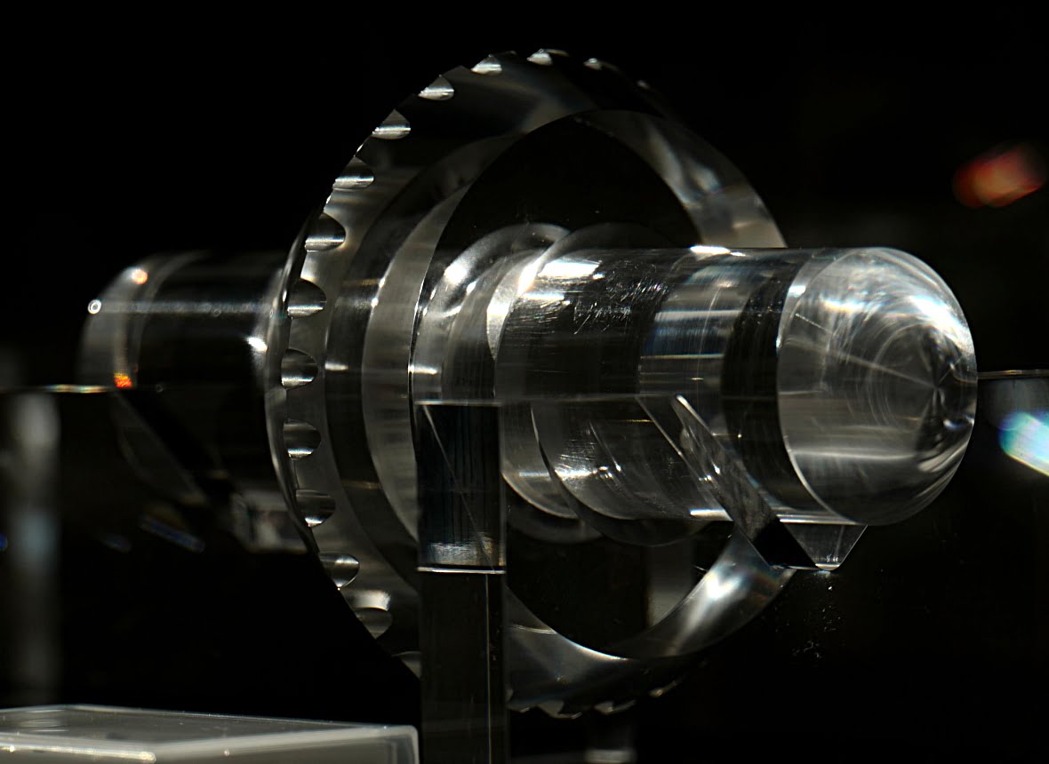
For many years, the company has applied its proprietary “Scribe & Break (SnB)” technology—refined through extensive experience in brittle material processing such as glass—to pursue high-productivity and high-precision wafer singulation in the semiconductor field.
With the recent expansion of the compound semiconductor market, including power semiconductors, production sites increasingly require flexible equipment capable of supporting various production scales and applications, ranging from research and development (R&D) to mass production.
The newly announced “DIALOGIC Plus+” is a completely new-concept wafer singulation system developed to meet these market needs.
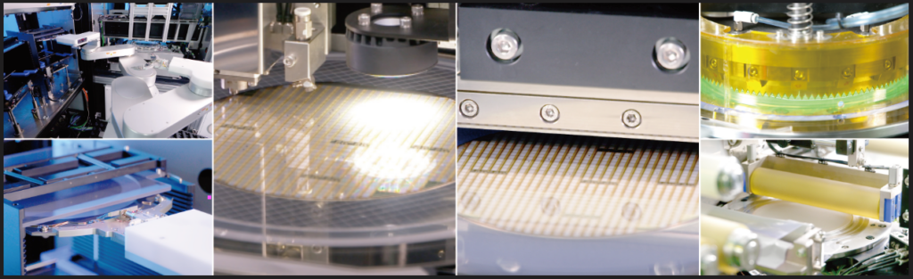
The greatest feature of this product is the modularization of each process incorporating our proprietary SnB method, enabling customers to freely combine modules according to their applications and production plans.
Key Features of DIALOGIC Plus+
Flexible customization and scalability through modularization
By configuring each SnB process as an independent module, the system seamlessly supports everything from R&D to mass production by adding and linking modules in line with future production plans. This approach optimizes customer investment and contributes to sustainable growth.
High productivity and quality through full automation
From cassette loading to protective film lamination/delamination, expansion, and remount, all processes are fully automated within the system. This automation minimizes operator error and achieves approximately 20% higher throughput compared to conventional systems.
High-quality singulation with proven SnB technology
The SnB method, proven effective for compound semiconductor wafers such as SiC, GaN, and GaAs, provides key benefits: less chipping, narrow kerf width, and a dry process that eliminates the need for water. These advantages enable the production of high-quality chips with high productivity.
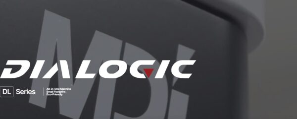
With its modular structure offering superior customization and scalability, “DIALOGIC Plus+” expands our product lineup alongside the well-received “DIALOGIC DL series” allowing us to provide optimal solutions tailored to customer production systems and needs.
Guided by our corporate philosophy of “Shaping the Future with Open Eyes,” we will continue to build on the processing technologies cultivated since our founding, contributing to innovation across various industries, including semiconductors.
Product Information
DIALOGIC Plus+ introduction site (Include Catalog Download):
www.mitsuboshidiamond.com/eng/dialogic-plus/
Contact Information
Mitsuboshi Diamond Industrial Co., Ltd.
Head Office: 32-12 Koroen Settsu, Osaka 566-0034, Japan
Website (JP): www.mitsuboshidiamond.com
Inquiries about the above products and services
To contact us through our website, please use the “Contact Us” button below.