Scribe dicing of compound semiconductor materials_SnB

SnB stands for Scribing and Breaking, a cutting technique that has conventionally been used for cutting brittle materials, such as glass.
This technique has also widely been used for cutting hard brittle materials, such as LCD glass substrates. We at MDI have extended the application range to singulation compound semiconductor materials by developing original scribing wheels and special laser optical systems.
What is a compound semiconductor?
It is a semiconductor made of two or more elements bonded together. As multiple different elements are combined, properties that cannot be achieved in a single-element semiconductor can be obtained. Furthermore, these properties can be regulated by changing the mixing ratio of elements. Making use of this advantage, many kinds of semiconductors have been produced.
《Combination of major compound semiconductors》
| II-IV compound | Cadmium telluride (CdTe), zinc selenide (ZnSe) |
| III-V compound | Gallium nitride (GaN), gallium arsenide (GaAs), aluminum nitride (AlN), indium phosphide (InP) |
| IV-IV compound | Silicon carbide (SiC), silicon-germanium (SiGe) |
These compound semiconductors are essentially covalent crystals, and many of them have a zinc blende structure or wurtzite structure. Gallium oxide (Ga2O3) is classified as an oxide semiconductor.
Features of SnB
(1) Minimal kerf loss
For SnB processing using a scribing wheel, the scribing groove width (part of plastic deformation area) is approximately 5 μm. This means that the street width can be reduced for semiconductor/electronic component substrates, and the number of chips per wafer can be increased accordingly.

(2) High-speed processing
SnB processing allows a scribing speed of 100 mm/s to 500 mm/s. Increasing the number of wafersto be processed per hour can reduce the number of machines required for production.
(3) Damage free
As SnB is a cleavage method, the only effect to wafers is processing marks caused by scribing. The cross-section forms a smooth cut plane, meaning that cracks are less likely to form on the cross-section, compared to other dicing methods, leading to higher bending strength of products (chips).
■ For materials with a crystal structure, the cross-section forms a cleavage plane, and the crystal structure is retained. Therefore, side cracks do not form.
(4) Dry process
Generally, large quantities of deionized water is required for semiconductor manufacturing processes, but SnB does not need any water as it is dry processing. This eco-friendly processing can save valuable water resources. There is no need to install incidental equipment to supply/drain washing water, leading to cost reduction.
MDI wheel scribing
About wheel scribing
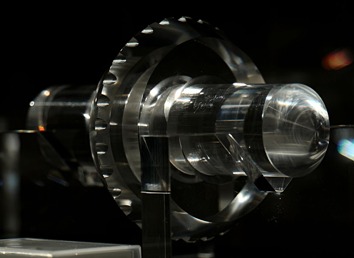
The scribing wheel applies pressure to the surface layer along the scribing line to create vertical cracks. This makes crack propagation possible by breaking.

Comparison with blade dicing, another mechanical processing

All scribing wheels are developed in-house and produced in the clean room at our factory.
An appropriate scribing wheel is selected according to the target material and product size.

MDI Laser scribing
MDI builds a laser engine optimal for substrate materials or product application quality and fabricates special optical systems to achieve the best laser scribing.

MDI has developed various laser scribing processes.
Heat stress crack propagation processing is a general technique where the material surface is heated by laser and then immediately cooled rapidly. Cracks propagate due to tensile stress generated in the cooling area.
BI (Brightness Innovation) processing performs spot laser processing at regular intervals on the substrate surface to form a vertical crack line through the linkage of cracks between processing points.
LMA (Laser Melting Alteration) processing irradiates the surface with a laser under ablation-free conditions to form an alteration layer by melting and cooling to form a stable vertical crack line.

In addition to these, non-scribing laser processing is available.
1-scan (entire thickness) processing is MDI’s original processing technique: Using a special optical system developed in-house, the surface is irradiated with a short pulse laser of a wavelength that penetrates the material to reform throughout the substrate thickness. Although the breaking process is still required, as is the case with SnB, 1-scan processing features high perpendicularity of the cross-section and high aspect ratio processing.


MDI Breaking
Substrates are diced by breaking. Specifically, the breaking bar presses on vertical cracks created by scribing from the rear surface to cut the wafer into pieces. Materials with a crystal structure take advantage of the substrate cleavage properties. Therefore, the cross-section forms a fine and smoothly cut plane (cleavage plane for crystal structure), meaning no cracks form on the cross-section.
■ As the crystal structure is retained, the cross-section forms not a mirror surface but an irregular surface according to the crystal structure.


SnB examples
Silicon carbide (SiC)
Thickness:0.36mm, Size:1.0×1.0mm

III-V compound:Gallium nitride (GaN)
Thickness:0.45mm

III-V compound:Gallium arsenide (GaAs)
Thickness:0.1mm, Size:0.7mm×0.75mm

III-V compound:Indium phosphide (InP)
Thickness:0.15mm, Size:0.4mm×0.4mm

Links to relevant pages
Inquiries Regarding the Above Products and Services
For inquiries via our website, please use the “Contact Form” available at the link below.

